There is no fundamental difference between creating a board and creating a macro. In this case, the same copper layers (M1, M2) are used for contact pads and conductors and silk-screen printing layers (K1, K2) for drawing projection lines of the component body. The application of the body projection is carried out using the simplest graphic elements (line, circle, etc.) in a silk-screen printing layer.
Example:
You need to create a macro for a 14-pin DIP package.
(This is just an example. It is quite natural that such a corpus already exists in the library.)
14 contact pads are applied to the M2 layer (bottom side) along a given grid (the grid pitch corresponds to the pin pitch). To identify the first pin, its pad can be made square.
Now you should make layer K1 active (silkscreen, top) and draw the outline of the body using the graphics commands. Additionally, you can mark a cutout on the body for better visualization.
So, the macro is almost ready.
Select a point on the working field with the cursor, press the left mouse button and, while holding it, mark the selection area. In this case, you should ensure that only those elements from which the macro is built fall into the selected area.

The selected elements will turn pink.

3. Saving a macro
To save the macro, selectSave as macro.. . in the menu File.
The same command is executed when you click the save button on the library panel.
This will open a dialog box. The save directory in it corresponds to the current library section. If you want to save the macro in another section, you must select the section accordingly.
The macro must be given a valid name. Macro file extension".lmk" (assigned by default to all macros) will be added automatically.
After saving the macro, it will be added to the selected library section.
Sprint Layout 6 Rus program
15200 macros for the program Program Sprint Layout 6 Rus
Video tutorial on working in the program Program Sprint Layout 6 Rus
Portable version
Very good and widespread amateur radio program for creating printed circuit boards. The program is Russified (very good translation), does not require installation on a computer (portable version). The program comes with more than 15,000 macros. The program archive is located on my Yandex Disk, you can download it from the link at the end of the article
This is what a printed circuit board might look like in Sprint Layout 6 Rus:

If you don’t know how to work in this program, then I suggest watching the video tutorial, which can be downloaded from the link at the end of the article: The video tutorial is also stored on Yandex Disk, file size is 99 megabytes, WMV video format, which allows you to view it in any video player.
The video tutorial was created based on version 5 of the program. In the 6th version, an interesting function appeared - loading a printed circuit board design, which is not suitable for manufacturing a printed circuit board using the LUT method (from a magazine article or book), and based on it, you can re-route the device tracks.
Procedure:
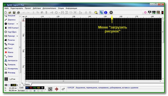
1. Place the cursor in the work field and right-click. In the window that appears, select the “Properties” menu:

In the window that appears, set the dimensions of the board; they are usually indicated in articles (for example, 70 by 45 mm).
2. Select the “Load drawing” menu, a window appears through which we load our printed circuit board drawing:

Usually the design of the loaded board does not fit into the dimensions we set (70x45).
In this case, in the “Resolution” column, increasing or decreasing the readings, we fit the downloaded drawing into our dimensions.

After all the contacts and tracks are drawn, through the “Load drawing” menu, simply delete the loaded drawing

Sprint Layout 6 RU
Sprint-Layout is easy-to-use software for creating single-sided, double-sided and multi-layer PCB designs. The program includes all the functions necessary to create a project. Even professional features are included, such as Gerber file export and Milling options
There are no restrictions or obstacles to creating a project. You can place pads, draw tracks, change layers, etc. however you want. You have full control over the project you create.
For each work operation, such as placing contacts, drawing paths or zones, adding text, etc., there are additional settings. Select the appropriate mode and configure.
Important parameters such as track width, court size or current grid setting are immediately visible and can be changed at any time. The integrated grid table can be disabled. By pressing and holding the CTRL key, you can change the grid spacing and add it to the table, if necessary.
You can modify and edit existing project elements. For example, select - Track and change width. All changes are immediately visible on the screen, so you can always evaluate the changes you have made.
There are functions such as copy, move, cut or paste, as well as rotate, flip and align functions.
Sprint-Layout has controllable layers, "K1" and "K2" - copper layers, "B1" and "B2" - component layers, for each side of the board (top and bottom). There is an additional “U” layer - contour, for the board layout, for cutouts in the board and the external contours of the board. If necessary, there are two additional inner copper layers I1 and I2, for a multilayer board. You can show or hide each layer. You can change the colors of layers.
The existing macro library already contains many standard components that can be placed in your project using the drag and drop method. If the required component is missing, there is no problem to create this component and save it in the macro library.
You can use the built-in auto-router to connect individual connections. But, Sprint-Layout does not automatically trace the entire project.
The photo-view function allows you to look at the created project as if it were real. This function allows you to find common errors, such as incorrect reflection of text or components.
Extensive and convenient printing functions allow you to print on paper or film, a drawing of a board or a plan for placing components on it.
You can export your project to BMP, GIF or JPG format. These images can be used in other programs such as Word or for publication on web pages.
Sprint-Layout can create Gerber and Excellon files for professional production of the project.
Milling is also supported. Sprint-Layout is able to generate the necessary data and export it to an HPGL file (plt). This file can be used with CNC milling software.
The Gerber import function allows you to load existing Gerber files and convert them into a ready-made project for Sprint-Layout.
New features of Sprint-Layout 6.0
Sprint-Layout graphics have been significantly improved through the use of anti-aliasing technology.
The resolution and accuracy of Sprint-Layout 6.0 are increased tenfold. This also applies to the grid parameters and maximum magnification. So, there are no problems in developing a very high-quality project.
Sprint-Layout allows you to manage components and display their details, including name and value. The components sheet is now available.
Sprint-Layout can now generate and export component data to a text file or pick+place file. These files are necessary for automated assembly of a board with SMD components.
The Gerber import function allows you to load existing Gerber files and convert them into a ready-made project for Sprint-Layout.
Multi-select - Edit multiple items at once
Using the properties panel, you can now edit many elements at once.
The new selector is a powerful tool. With this tool you can find and select specific elements of your project, and edit them simultaneously using the new multiselect function. For example, you can select and edit all pads with a specific shape or hole.
This new auto-grip mode makes it easier to connect pad and track. When you draw a path and the cursor is exactly in the center of the pad, the contact will be captured. At this point, the cursor will be highlighted with a red crosshair, allowing you to connect accurately. This is useful if some pads are not on the grid.
When you move elements connected by tracks, they retain their connections, which stretch like an elastic.
New mode rectangle, allows you to easily draw rectangles (outline or polygon with fill).
Keys 1..9 on the keyboard are now hot keys for quickly setting the grid spacing. You can immediately change the grid spacing with just one keystroke.
The new crosshair is constantly involved in every action. It displays additional 45 degree lines and numerical coordinates directly on the crosshair.
It is difficult to arrange the elements exactly in a circle. Now Sprint-Layout has a special assistant for this. You just need to define the necessary parameters, and you can see the result before completing the action.
If you are using vias as a thermal barrier, you can now define the thermal barrier separately for each layer.
Milling, completely revised. All individual work actions, such as route milling, drilling and cutting, will now be recorded in one plot file. Errors with file compatibility are now eliminated.
...and other improvements
Workspace properties
Starting with a new project, the first step is to determine the dimensions of the working area. Select the command from the main menu File | New...

If you want to create your project without any template, then select the first option: Empty workspace without board outline.
The other two options allow you to choose between a rectangular or circular board outline. The board outline will be generated automatically, according to your parameters, using the outline of the -layer (U).
The working field cannot be larger than 500x500 mm. You can change these settings as you wish.
Select New | Properties... or right-click, call the command from the -Board tab (at the bottom of the working field).

The properties panel will appear on the right.
Now you can change the size of the working area or the name of the project.
The Multilayer function offers 2 additional internal layers I1 and I2, for creating multilayer PCBs.
Setting Grid Options
One of the most important features of Sprint-Layout is the grid option. The grid allows you to quickly and accurately place all elements. The grid is always active and displayed on the screen. If the selected scale is too small to display the grid on screen, the grid is not displayed, but even then, snap to grid is still active.
You can change the grid size. Changing the grid size will not affect the generated project. If you cannot achieve the desired position of the element on the board, then you need to reduce the grid size.
Tip: You can turn off snap to grid at any time. Simply press and hold the CTRL key while moving or drawing elements.
You can set any grid size value. But in most cases, it makes sense to set the default grid size to 2.54 mm (1/10 inch). To adjust the grid size, click on the corresponding button in the left sidebar:
A menu will appear to set the grid size.
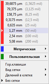
The top red entries are the default values in inch format. Open the metric grid and select a new grid size in metric format. Open Custom Grid and set a custom grid size that can be added to the list, or select a grid size from the list.
Hotkeys...
1..9 keys on the keyboard are hot keys for special grid sizes. You can change the grid size with one press of one of these keys. Here you can define the grid size for these keys:

Auxiliary functions
By default, every 5th grid line appears thicker than the others. This is often useful for orientation. This submenu allows you to configure or disable this feature.
Show grid
With this function, you can show or hide the grid.
Note: Even if you hide the grid, snap to grid is active.
Purpose of layers
Sprint-Layout 6 supports up to 7 different layers. You can think of the layer as a transparent film. You can overlay several layers, one on top of the other, and view all layers at the same time.
Each layer has its own purpose:
K1= top copper layer.
B1= layer with upper components (installed on the side of the copper layer K1).
K2= bottom copper layer.
B2= layer with lower components (installed on the side of the copper layer K2).
U= contour layer, for the outline of the printed circuit board and all kinds of cutouts.
I1= copper - inner layer 1 (only for multilayer boards).
I2= copper - inner layer 2 (only for multilayer boards).
2 layers for the top and bottom sides of the board. One copper layer for drawing the design (contacts, tracks, polygons, etc.), and one additional component layer for creating a component layout plan.
You can use the U outline layer to define the edges (borders) of the board, various cutouts in the board, etc. It can be a simple rectangle or a complex shape with several slots. Simply draw thin line outlines or circle segments on the U layer. Contour U-layer can be used for professional production project.
Please pay attention to the following points when you start drawing the board:
Side 1 is the top of the board.
Side 2 is the BOTTOM of the board.
Always design from the TOP side, and look through all the layers as if the board were transparent.
Important - each text or component on the BOTTOM side must be mirrored. (Sprint-Layout does this automatically).
All new drawing elements will be inserted into the current active layer.
At the bottom of the working field, in the Sprint-Layout window (status bar), you can view or change the active layer:
![]()
Buttons for selecting the active layer.
You can hide a layer using the buttons K1, B1, K2, B2 and U, above the round buttons that switch the visibility of the layer. Note that the active layer is always visible. By pressing the F9 key, you can toggle the activation of only layers K1 and K2.
Using a button ? You can see information about layers:
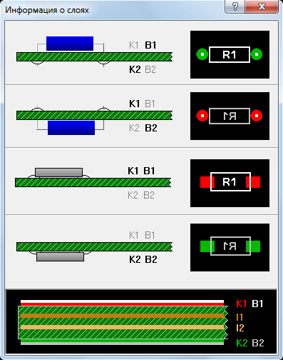
This window explains the purpose of layers and their colors.
Rulers and coordinates
Sprint-Layout 6 has two important functions for better orientation in the workspace:
Rulers
The rulers are located on the top and left borders of the working field. The current cursor position is marked on them with red lines for better orientation.
You can change the ruler units from millimeters to mil (1 mil = 1/1000 inch). To switch units of measurement, click on the small button at the top/left edge of the rulers. The current units are always displayed on this button.
Coordinates
The coordinates are displayed on the left side of the status bar, at the bottom:
The coordinate units correspond to the ruler units.
Origin
Typically, the origin is at the bottom/left side of the workspace. Sometimes it is necessary to change this situation. Important - if you selected a board outline template, the origin of coordinates will be set to the lower left side of the working field:

The cursor appears as a crosshair. Click the mouse button and move the cursor to a new position.
Clue:
When moving, the cursor will be displayed on the working field grid and linked to it. You can press and hold the CTRL key to turn off snap to grid and move the cursor to a position outside the grid.
Working with multiple work fields
A Sprint-Layout file can contain multiple project sections. This can be useful when you need to save a project with several boards into one file. In this case, you have access to all sections of the project saved in one file.
Each section has its own tab at the bottom of the workspace:

Just click on the tab, select the project section. You can change the order of these boards, or add new boards from other Sprint-Layout files. By right-clicking on a tab, you can call up a pop-up menu with the following functions:
(You can call these functions from the main Project menu)
New board ( new project)... This function adds a new, empty workspace for creating a project.
Workfield (board) properties. This function shows the workfield properties panel on the right side. Here you can edit the workspace size, project name, etc.
Copy the board. This function copies the currently selected section and adds that copy to your project.
Remove PCB (Workspace)... This function removes a PCB from your project.
Sorting tabs. There are 4 functions to change the order of project sections:
Set to Right - Moves the tab to the right edge
Set to Left - Moves the tab to the left edge
Move right – the tab moves one step to the right
Move left – the tab moves one step to the left
Importing boards from a file... You can import projects (boards) from other Sprint-Layout files. These projects (boards) will be added as new ones to your project. To import boards from another Sprint-Layout file, in the main menu click on Project | Import from file... . If you don't want to add all the boards from another file, simply remove the unnecessary tabs after importing them.
Basic PCB Drawing Functions
Each of these functions has its own drawing mode. You can select the drawing mode in the left sidebar.
Enter edit mode if you want to select, edit, or move items.
To switch to editing mode, you need to select an element, and in the main menu, click Actions. To exit the mode, you can right-click on the workspace, or press the ESC key.
Advice:
You can quickly switch to editing mode by placing the cursor on the selected element and right-clicking. The window that opens will give you quick and convenient access to frequently used functions.
Selection and highlighting
Once elements are created, they can be edited. You can move, delete, copy, and edit these items. To change an element, select it. Simply, hover over the element you want to edit and click. The element will change its color to pink. This color always identifies the selection of elements. To deselect and highlight selected items, simply move the cursor over an empty space and click the mouse button. The items will be deselected immediately.
If you want to select several elements at the same time, you can select a group of elements with a rectangular frame. Imagine a selected area of a group of elements, move the cursor over an empty space in any corner of the imaginable area, click the mouse button and, while holding the button, move the cursor, highlighting the selected group of elements, release the mouse button. All or part of the elements that are inside the dotted frame will be selected.
If you want to select multiple individual items, you can use the SHIFT key. Press and hold the SHIFT key, you can now select one item after another without deselecting previously selected items.
Advice:
If you want to select one element from a grouped component or macro, press and hold the ALT key, and hover over the desired element and click the mouse button.
You can combine all of these features to create a more complex selection.
Moving
Select the items you want to move. Then move the cursor over one of the selected elements and hold down the left mouse button. Move the elements to the desired position and release the mouse button to lock them. You can also use the ARROW keys on your keyboard to move selected items.
Advice:
If you need to install an element outside the grid, i.e. without snapping to grid, press and hold the CTRL key on your keyboard to turn off snapping to grid. Move the selected elements as described above.
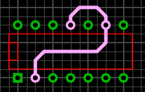
Paths and lines
To draw copper traces, select the appropriate mode from the left sidebar:
When you move the cursor to the work field and click the mouse button, you will see additional data for moving the track. This item defines the starting point of the new track. Click the mouse button to confirm the starting point. Having determined the starting point, regardless of whether you are drawing a straight or broken line, each click of the mouse button fixes the end point of the drawn segment and determines the beginning of a new segment, the data indicator is reset to “0”.

If you want to finish drawing, just RIGHT click. Now you can start drawing a new path. If you want to exit Explorer mode, simply RIGHT-click again, or press
Bend
While drawing a path, you can change the drawing mode. When bending, you can draw a path in a straight line, at any angle, or only at a right angle. This mode can be changed by pressing the key<ПРОБЕЛ>. In general, there are 5 modes, and these modes are switched using the key<ПРОБЕЛ>.
Advice:
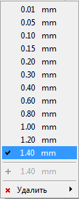
The current track width is displayed in the left panel next to the width button:
Here you can change the current track width. Width "0" is always displayed as the thinnest line and is supported by devices (screen or printer). There is a list available for commonly used track widths. Click on the symbol in the left panel:
A pop-up list will appear in which you can select the desired width with one click of the mouse:
+ Delete .
To change the existing width, select a track:

Track nodes appear as round blue dots. You can click on a node and drag it to a new position. Virtual nodes are located in the middle of each track segment, and are represented by a blue circular outline. Drag them to a new position to create new nodes. This makes editing tracks easier.
If you RIGHT-click on a node, a pop-up menu will appear that allows you to delete the node, adjust the node(s) to a grid, or split the track into 2 separate tracks.
Whenever you select a track, the track width is displayed in the wire width box in the left panel:
You can adjust the width for the selected track (and for all tracks that are selected). Whenever a track is selected, the width will be displayed in red. This shows the existing width of the selected track, and means that any changes to the width of the selected track are now available.
Contact pads, transition contacts, holes
Select the appropriate mode from the left sidebar:
Sprint Layout offers several pad shapes. The selected form will be displayed on the button. To select a different shape, click the arrow to the right of the button.
If the WITH METALLIZATION option is selected, pads will appear on both sides of the board automatically (on multilayer boards they also appear on the inner layers I1 and I2). These areas (with metallization) are indicated in a different color. You can quickly apply/cancel the "With metallization" option by pressing the F12 key.
Move the cursor around the work area. Each mouse click adds a pad to the project.

The “Contact” mode can be interrupted by pressing the right mouse button (or

Note:
Pads with simple holes are not reflected on other layers. You can connect them, but the hole will not be metallized.
Advice:
Hold down the CTRL key on your keyboard to turn off snap to grid if you want to set it to an off-grid position.
The current size of the pad and hole is displayed in the left panel near the mode button:
Here you can change the current values. For commonly used pad sizes, there is a list available. Click on the symbol in the left panel:
A menu will appear in which you can select the required size of the site with one click:

If the required value is not in the list, you can add it to the list using the " + ". If the current value is already in the list, it will be marked and there will be no entry. You can delete unnecessary entries with the option Delete .
The current size of the selected contact is displayed in the left sidebar. The form will also be displayed on the mode button:
You can choose a different shape or size for the pad and the hole in it. If multiple pads are selected, changes will be made to all selected pads.
When a pad is selected, the size will be displayed in red. This indicates the current size of the pad and its opening, and that changes are available.
By right-clicking on the selected contact, you can call up the menu and select “Properties”. The Properties panel will appear and you can edit it:

Clean hole.
Clean hole, without any copper ring. These holes are typically used to secure component housings to the board, or to secure the board itself. Set the same values for the inner diameter and outer diameter of the pad for the hole without copper. Such holes are designated as a cross.
Transition contact (with metallization)
A transition contact (also called plating) appears on both sides of the board automatically. The transition pin is used to connect the trace on both sides of the board. The transition contact is indicated by a special color.
To place a contact with metallization, select the With metallization option from the Contact button pop-up menu by clicking the arrow next to the button. Drawing and editing transition contacts, like regular pads.
You can select existing pads and change them by entering the menu and selecting With metallization, or by right-clicking on the selected contact, selecting “Properties” from the pop-up menu, and changing the contact values in the properties panel.
Advice:
It is possible to change a simple contact into a contact with metallization, and vice versa. Select the contact(s) and press the key
Thermo contact (thermal barrier)
This Thermal Contact option is available if the function of auto-filling free areas of the board with the GND layer is enabled. The thermal contact looks like this:
The thermal contact is more sensitive to heat because it is not completely surrounded by copper. Additional properties for thermal contact:

You can change the width and position of the small tracks that connect the thermal contact to the ground layer. If thermal contact is with metallization, it is possible to change the position of small tracks for each layer separately. To do this, select the layer. The settings are valid only for the currently active layer. Thus, by changing layers, we set the thermal contact parameters for each layer.
SMD contacts
In the left panel, select SMD-Pin mode:
Move the mouse cursor to the work area. Each mouse click adds an SMD contact to the project.

3 different SMD pins
Advice:
Hold down the key
The current size of the SMD contact is displayed at the bottom of the left panel, near the mode button:
Click on the small arrow on the edit button, a pop-up list will appear with dimensions for both values of the SMD pad. For commonly used SMD pad sizes, there is a list of available sizes. Click on the symbol in the left panel:
A menu will appear from which you can select the desired size with one click:

If the required value is not in the list, you can add it to the list using the " + ". If the current value is already in the list, it will be marked and there will be no entry. You can delete unnecessary entries with the option Delete .
To change an existing SMD contact, select SMD Contact. When an SMD pin is selected, its size is reflected in the window next to the edit button at the bottom of the left panel.
You can customize the size of the SMD pad. Changes will be made to all selected SMD contacts, if more than one contact is selected. When an SMD pad is selected, its field size will be displayed in red. This shows the current value of the site, and means that any changes to these values are available.
Circle/Arc
To draw a circle, select the appropriate mode in the left sidebar:
Click the mouse button on the working field to determine the center of the circle and draw a circle of the desired size while holding the mouse button. The width of the circle line corresponds to the current track width setting.
The mode can be interrupted by pressing the right mouse button (or
Advice:
Hold down the key
The current width of the circle line is displayed in the left panel near the line mode button:
You can change the current circle line width.
Width "0" is always displayed as the thinnest line supported by the devices (screen or printer). The line width of the selected circle is displayed in the window next to the line editing button in the left sidebar:
You can adjust the line width for the selected circle (and for all other selected circles). The line width of the selected circle will be displayed in red. This shows the current circle line width and indicates that changes are available.
You can leave an arc (segment) from the circle. To do this, there are two points on the circle that define the beginning and end of the arc (segment). Both points are aligned and are at the 3 o'clock position (meaning 0 degrees). You can move these dots (shown as blue dots) to your desired position. You can change the diameter of the selected circle. Press and hold the key
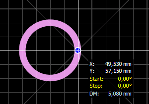
Setting up a circle or arc in fixed numbers can be done in the Properties Panel. Select a circle. Select it with the right mouse button. In the pop-up menu, select “Properties”, and in the window that opens, edit the properties of the circle:
Rectangles
To draw a rectangle, select the appropriate mode in the left sidebar:
Click the mouse button on the working field to determine the starting point of the rectangle, and while holding the button, draw a rectangle of the desired size. The line width of the rectangle corresponds to the set line width.

The mode can be interrupted by pressing the right mouse button (or
Advice:
Hold down the key
The current line width of the rectangle is displayed in the left panel near the line editing button:
You can change the current line width of a rectangle. Width "0" indicates the thinnest line supported by the devices (screen or printer).
Filled rectangles
Click the arrow on the right side of the mode button in the left sidebar and select Filled.

A rectangle can be created as an outline or filled (like a polygon).
Zones/polygons
The filled areas are called polygons. The polygons on the copper layer associated with certain signals are called power polygons (Zone/power polygon, GND polygon/ground, etc.). The zone outline is drawn in the same way as tracks; when the outline is closed, the polygons are filled automatically.
To draw a polygon, select the appropriate mode in the left sidebar:
Place the cursor on the work field, you will see an additional dot with a size corresponding to the set track width. This point defines the start of drawing the zone. Click the mouse button to confirm the starting point. Move your cursor and draw a zone. Each mouse click leaves an additional node on the zone outline, which makes editing the polygon easier. Close the loop.

To finish drawing, click the RIGHT mouse button. Now you can start drawing a new outline. To exit the mode, click again with the RIGHT mouse button, or press the key
The closed loop is filled in automatically. Please note that you will need at least three points for one zone. Otherwise the zone will not be created.
Bend mode
While drawing a zone outline, you can change the bend of the line by pressing the key<ПРОБЕЛ>. There are 5 modes, they can be switched with a key<ПРОБЕЛ>.
Advice:
Hold down the key
The current width of the zone contour line is displayed in the left panel, near the line editing button:
You can change the current zone boundary line width. To modify an existing polygon, select it:
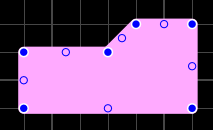
Zone nodes will appear as round blue dots. You can click on a node and drag it to a new position.
Virtual nodes
These nodes are located in the middle of each line segment. Drag them to a new position to create new nodes.
Place the cursor on a node and click the RIGHT mouse button, a pop-up menu will appear that will allow you to various actions with a knot.
The track width of the selected zone is displayed in the line width box next to the edit button in the left sidebar:
You can adjust the line width for the selected zone (and for all other zones that are selected). The width of the contour line of the selected zone will be displayed in red. This shows the current line width and means changes are available.
If the Properties Panel is enabled, you can make some additional settings:

Polygons can be solid or with a grid. Select an option With mesh and set the grid size.
Special shapes
You can create various geometric shapes:
Polygons
Layout form
Polygons can be useful for creating a project. For example, if you want a component with 12 pins arranged in a circle, you can create a 12-gon polygon, place a pad at each corner, then delete the polygon outline. Spirals are mainly in demand on RF boards. To create a custom shape, select the appropriate mode in the left sidebar:
Create a polygon

Confirm by clicking OK, the polygon will be placed on the workspace. Move the cursor to select a position to place the polygon. Left-click to confirm and fix the polygon on the workspace. When you have confirmed your choice by clicking OK, and the figure appears on the work field, you can cancel this action by right-clicking. You can exit the mode by closing the mode window, or by pressing the key
Create a spiral
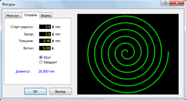
You need to set the necessary parameters. The specified parameters are always visible in the preview window.
Confirm by clicking OK, the spiral will be placed on the workspace. Move the cursor to select a position to place the spiral. Click the left mouse button to confirm and fix the spiral on the working field. When you have confirmed your choice by clicking OK, and the figure appears on the work field, you can cancel this action by right-clicking. You can exit the mode by closing the mode window, or by pressing the key
Create a layout form

You need to set the necessary parameters. The specified parameters are always visible in the preview window.
Confirm by clicking OK, the form will be placed on the workspace. Move the cursor to select a position to place the form. Left-click to confirm and commit the form to the workspace. When you have confirmed your choice by clicking OK, and the form appears on the work field, you can cancel this action by right-clicking. You can exit the mode by closing the mode window, or by pressing the key
Advice:
Hold down the key
Select the appropriate mode in the left sidebar:
The following dialog box will appear:
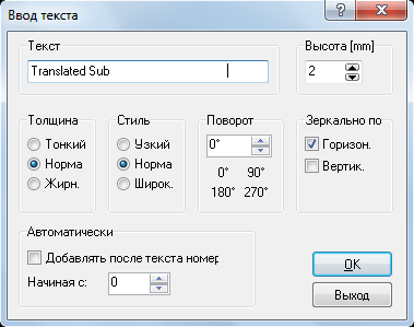
You can enter text and set additional options such as height, style, orientation, etc. Russian letters are NOT supported when entering text!!!
After confirming the selected parameters, move the cursor and place the text, clicking the left mouse button to fix the text in the selected position. Text mode can be interrupted by pressing the RIGHT mouse button (or
Advice:
Hold down the key

2 texts above and below. Text on lower layers (K2 or B2) should always be mirrored. When you look at the photo view of the board, you will see a mirror image of the text. Sprint-Layout does the mirroring automatically.
Automatically
With the Automatic function, you can create text labels with sequential numbers (like R1, R2, R3, ...). The number will be added to the text automatically. After placing the first text, you can immediately and quickly place the next text with the next number. You can interrupt automatic mode by pressing the RIGHT mouse button (or
To change existing text, double-click on the selected text with the left mouse button, and in the window that opens, you can change its parameters. If the properties panel is visible, you can edit the text directly in it::
Using the clipboard
The clipboard is a very useful tool in almost any windows application. The clipboard is a container that can be used to copy project elements. The clipboard uses the following functions:
Cut
Copy
Insert
Duplicate
These commands are in the top menu. Each command has a button on the toolbar. These commands are also available in pop-up windows.
Copies selected elements of your project to the clipboard. After this, the selected elements will be removed from the project.
Copies selected elements from the project to the clipboard.
Copies the contents of the clipboard to the project.
The clipboard elements will be, as it were, “glued” to the mouse cursor. You can put them in one click with the mouse button.
Performs COPY and PASTE in one step.
The zoom function is a very important feature of Sprint-Layout. Only this function makes it possible to view the complete project, as well as the allocated space, in a large format. Zooming using the mouse wheel is the easiest and most convenient way to zoom in and out.
If the mouse cursor is on the working field, you can zoom in or out using the mouse wheel. You can freely move the cursor around the work field. When zooming in, the cursor position is the center of the enlarged project. You can increase or decrease it a little.
All other possibilities for increase are outdated and not rational, but, nevertheless, they are possible:
Zoom mode
To adjust the scale, click on the corresponding button in the left sidebar:
The mouse cursor will change to a magnifying glass (magnifying glass). Left-clicking zooms in and right-clicking zooms out. You can highlight the selected area with a dotted frame to enlarge it.
There are additional zoom functions that you can use in the toolbar:
Returns to the previous scale.
Adjusts the scale so that the board is displayed on the entire screen.
Adjusts the scale so that all objects fit on the working field.
Adjusts the scale so that all selected objects fit on the working field.
Additional zoom function
In addition to the normal zoom function, you can use the Show Zoom Change function. You can activate or deactivate this feature in the general settings menu. Sprint-Layout. If the feature is enabled, it will appear in the left sidebar:

Dark green color panel symbolizes the full working field (screen), and the light green color of the panel symbolizes the viewed area. Place the cursor on the light green panel, press and hold the left mouse button, and move the cursor. In the workspace, you will see the viewing area move. This way you can “travel” and view the entire project.
By placing the cursor on the light green panel, clicking the left or right mouse button, you can change the scale:
Click the left mouse button to enlarge the project image on the workspace, and the light green panel will become smaller
Right-click to zoom out the project image on the workspace, and the light green panel will become larger
It is not necessary to select this function. You can use any scale mode separately in each case.
Rotate, flip, combine
You can rotate, mirror, and align any element in your project.
Functions used:
Rotate (rotate)
Mirror horizontally
Mirror vertically
Combine
Snap to Grid
You can find these commands in the Actions menu. Each function has a button on the toolbar. You can see these commands in pop-up windows.
Rotate (rotate). This function rotates all selected elements clockwise by specified angle. Click on the small arrow to determine the desired rotation angle. You can rotate both individual elements and a group of selected elements.
Advice:
If you press the SHIFT key, the selected item(s) will rotate counterclockwise.
These features mirror selected items, both vertically and horizontally.
This function configures all selected items. You can align to the top edge or bottom. Align left or right, horizontally centered, or vertically centered.
This function snaps to the grid the positions of all selected elements. Note: This may change the spacing of elements not grouped together. The position of elements that are grouped together will not be affected. Grouped elements are shifted by the entire group.
Group and Ungroup
Project elements can be combined into groups. Combining elements into a group is easy, using a single operation. Grouped elements are protected from unwanted changes. You cannot delete a single element that belongs to a group. At least two elements are required to create a group. Groups can contain any project elements, even other subgroups.
To remove or change individual elements of a group, you must first split the group. When a group is divided, all elements and other subgroups are independent. The subgroups remain ungrouped, but you can repeat the operation and separate the subgroups.
Advice:
You can select one element from a group, press Alt and click on the element to select it.
You can Ungroup or Group from the Actions menu, or using the corresponding buttons on the toolbar. These functions are also available from pop-up menu windows (right mouse button).
Sprint Layout 6 groups elements automatically if they were pasted from the clipboard or macro library. This allows you to place elements as one unit. You can separate these groups, as well as any other subgroups.
Connections
You can connect pins or SMD pins of the project. This can be useful to remember to draw a path.
Relationships are very important for working with integrated Autorouting. The highway uses these connections to draw tracks.
Connections are displayed as thin, establishing lines, which is also useful when choosing the appropriate position of a component. You can use them to avoid crossing traces when placing components on the board.
Select the “Communications” mode using the corresponding button in the left sidebar:
One connection can only be made between 2 pads or SMD contacts. Hover your cursor over the first pad you want to connect and click. After this, move the cursor to the second platform to which you want to connect and click the mouse button. The link appears yellow while the cursor is moving. dotted line, and upon completion, a thin line of a given color. The pad lights up when you hover over it to make connections easier.
Right-click to abort the process.

Example: 3 connections
Remove existing connections
To delete an existing connection, you must activate the connection. Move the mouse cursor over an existing connection, the pad will be highlighted pink, click on the highlighted contact with the left mouse button and move the cursor to another communication contact, it will also be highlighted, click on it. The connection will be deleted.
Sprint Layout has another feature for deleting links. This makes it possible to delete connections automatically, or by simply hovering the cursor over the communication line, without moving from one contact to another. You can call the Delete virtual connections function from the Advanced menu, or using the corresponding button in the toolbar.
This function checks every established connection and removes it. Sprint Layout also checks and removes connections between different layers of a double-sided board. The function will inform you when the removal process is complete.
Auto-trace
The auto-routing function is integrated into Sprint-Layout. Autorouting can connect two pins in a project. These two contacts are defined by connections. Auto-routing is not intended to create an entire project at once. Usually this is not possible. To create a proper project, you must first create it manually by establishing connections, then enable the autorouting feature.
The project is created by a simple autorouter. You cannot set complex parameters and connections.
To use auto-trace, select the appropriate button in the left sidebar:
This small panel appears at the top of your project:
You can set the width of the track that will be used for auto-routing and define the minimum distance to other project elements that will be taken into account when laying the track.
Orientation according to the current grid:
This additional auto-routing option uses grid snapping when drawing tracks. The current autorouting mesh will be displayed below this option.
Automatic link routing
Select the desired connection using the mouse. When the cursor is placed on a connection, it will be highlighted. By clicking the mouse button, you can autoroute this connection.

Example: 2 highways
Autotracing will be done on the active layer. Make sure the desired layer is activated.
The autorouter searches for the shortest path to draw the track. It respects the given minimum distance between elements along the path:
Elements on active layer
Holes
If the autorouter finds a path, the path will be drawn. Otherwise, you will receive a message in the tracer panel.
Highways are marked with an inner lane. You can distinguish between highways and simple paths.
Cancellation of the highway
You can return the traced path back to the connection. Just click on the highway and get the original connection.
Change highway
You can edit a traced track as you would a regular track. You can adjust the width, change the bend, etc.
Tips for using the autorouter
If there are many connections along the route, autorouting starts with the shortest and simplest connection. If you find that one highway is "blocking" some other routes for other connections, cancel that highway and try the other connections first. Vary the connection sequence to get better results.
The autorouter can find a route more quickly if the track width and distance are not large. Try changing these values if the autorouter does not find the connection route. In any case, you can change the highway, if necessary, manually.
Function - Test
This is a very useful feature for checking electrical connections in a project. Sprint-Layout can find the connection of pads with traces to other elements of the project. Place the test cursor over the element being tested and click the mouse button; all elements associated with the element being tested will be highlighted.
Enable test mode using the corresponding button in the left sidebar:
The mouse cursor will look like a pointer with a cross and the words “test”. Hover the test cursor and click on any element and Sprint-Layout will find all the tracks, pads and other elements that are connected to this element. You can test connections on both sides of the board without changing the active layer. You can click the button on another element, or cancel the test mode using the RIGHT mouse button, or by pressing the key
Note:
The test will also look at connections that are made using plated vias (vias) on the opposite side of the board.
Flashing test mode
Connected elements can be displayed in flashing mode. This will help determine the connection of the elements. You can enable or disable flashing mode in the general settings of Sprint-Layout.
View all connections in test mode
You can define an option so that all connections are considered in test mode, including connections (virtual connections). In this case, all elements that are connected by links will also be recognized as “connected”. You can set this option in the general settings of Sprint-Layout.
Mode - Measurement
With this function you can measure distances and angles in the created project. To select a measurement mode, click on the corresponding button in the left sidebar:
Move the cursor over the work field, click the mouse button and draw a frame:
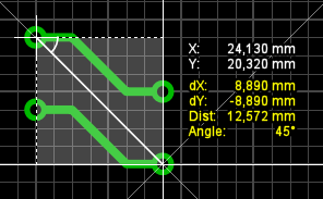
You will see the following values:
X: X-Coordinate
Y: Y-Coordinate
dX: Distance in X direction (horizontal distance)
dY: Distance in Y direction (vertical distance)
Dist: Absolute distance (diagonal distance)
Angle: Angle of deviation from horizontal
With these values you can accurately measure the distance and angle in your project. Measurements will be more accurate with a larger scale.
You can exit the measurement mode by clicking the RIGHT mouse button (or pressing
Advice:
Hold down the key
Automatic installation "GND - ground"
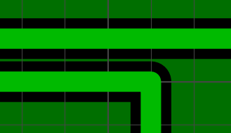
This feature automatically fills unused areas of the copper layer on the board. This speeds up the board etching process and saves etching solution. You can use this function to create a shield for the RF board. Please note that the function creates a space that is NOT associated with any project signal. So, you will have to connect these areas to GND (ground) yourself if necessary.
"Automatic ground" is available for each copper layer of the board. To enable or disable this feature, click on the corresponding button at the bottom of the editor panel:
A window will open:
"Auto Ground" is enabled for the active layer and will appear on your workspace. You can turn this window on/off whenever you want without any loss of information.
You can adjust the distance between the “ground” and existing paths, platforms and other elements. The distance is adjusted for each design element in the input window to the right of the "auto-ground" button (only if the "ground" plane is activated). To change the distance of an existing element, select the element and then change the gap value between it and the ground layer. The result is immediately visible on the project.
Advice:
If you set the gap to "0", the element will be in contact with the "ground" layer. So it's possible to set pads or trace edges to the ground layer that are connected to the ground.
Cut out areas
You can create cut out areas. These areas will NOT be filled by the auto-land feature.
To create a clipped area, move the cursor over one of the shaded areas shown next to the "auto ground" button. The shaded areas are shown immediately below the digital gap setting window. The left figure is to cut out a rectangular area, the right figure is to cut out a broken area. Left-click to select the shape of the cut area. Move the cursor to the activated “ground” layer, left-click, and start drawing the area that needs to be cut out. You can create one or more clipped areas on the ground layer. You can edit the cut out areas just like regular rectangles or zones.
Attention:
Depending on the distance between traces and contacts, auto-generation of the ground may lead to thinning of the copper in some places. In this case, these sections of copper may become detached from the board and cause a broken connection. Or narrow areas will not be able to “survive” the etching process, there will be so-called “undergrasses”, which will also lead to loss of connection.
Pattern: Narrow copper areas between traces
Check the project for such areas when using this function. To avoid tight copper areas, move the traces to a different location, change the distance to ground, or use cutout areas.
You can upload a bitmap image as a background for your project. This bitmap image could be a scanned copy of another project. You can use this bitmap as the original to make a board.
The raster image must be in the form of a graphic file (BMP or JPG). The resolution should be between 300-600 dpi. Recommended, but not required, color B/W.
Upload a bitmap image for the background
Select the Load picture... command from the Advanced menu, or click the corresponding button on the toolbar:
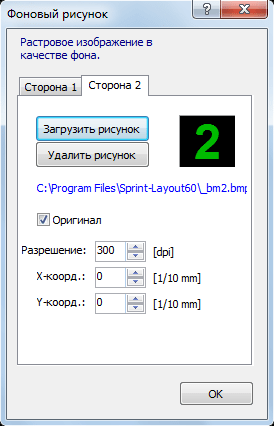
Board Side 1 (Top) / Board Side 2 (Bottom)
You can select the desired side for the bitmap image.
Upload drawing...
Opens a file selection dialog, select an image file. The image file must be in BMP or JPG format.
Delete Picture - You can delete the downloaded wallpaper.
Original - This option shows or hides the loaded background image.
Resolution - Sprint-Layout attempts to detect the resolution of the raster file automatically. But, unfortunately, in some cases this value is not suitable for recognition by the program, and the program cannot recognize and load the picture correctly. If the bitmap image is not displayed at true scale, you will need to change the resolution values until the image appears at true scale.
X/Y coordinates - you can define coordinates to position the image on the board. Adjust these values to get the correct position in relation to your current grid.
You can call this dialog box at any time to change these settings.
Project from the original
If you want to create a Sprint-Layout file from a scanned copy of an image, upload the image file in the background and then draw the image manually. Make sure the image is displayed at the correct scale. To adjust the X- and Y-coordinates, we recommend a small grid step, with a small number of divisions in the main cell (the default is 2 or 4 divisions), and a high magnification. Try moving the image to a position that fits on the grid in the best possible way. Try different grid spacing and magnification to draw details of the design that are outside the grid. For objects that are completely off the grid, you can use the CTRL key to temporarily disable snapping to the grid.
When the background image is loaded and visible on the workspace, 2 additional buttons will appear at the bottom of the editor. Attention! Don't forget to activate the layer on which you loaded the drawing (in the status bar, below).
Using the Exclusive button, you can enhance the image. The Hide button allows you to temporarily hide the image (for as long as the Hide button is pressed). This option helps maintain clarity in some cases.
Cascade / Cascade in a circle
Using this function, you can copy elements and place them in a cascade, both horizontally and vertically, as well as in a circle.
Select the desired element, then select “Actions” from the menu, or RIGHT-click on the selected element, and select the command Cascade / Cascade in a circle.

Enter the required number of horizontal and vertical copies, as well as the distance between them.
The entered parameters are always visible in the preview window.
Click OK, the action will be executed and you will see the result in your project.
Cascade in a circle

Quantity
Total number of copies.
Angle between individual copies..
The radius of an imaginary circle for placing copies.
Rotate elements
This option determines whether the copied elements should rotate themselves, relative to the center of the circle, placing their axis along the radius line.
Arc starting point
The starting point of an imaginary arc centered on the element being copied (0/0). You can change this point to another position. You can set the starting point at the center of the site, i.e. return to original position. You can select the desired copy of the element, snapped to the center, using the 2 arrow buttons.
Once you have entered the specified parameters (number, angle, radius, arc starting point or center), confirm by clicking OK. The created copies will appear on the working area and will still be selected. You can change them, edit them. To edit, call the “Cascade in a circle” command again, this window will appear again, where you can change the parameters, select any of the available copies and make it central (snap to the center), change the position of the center relative to the selected copy.
Click OK, the action will be executed and you will get the result in your project.
The photo view allows you to look at the project as if it were already made, with holes, components, etc.
This will help you find common errors like incorrect mirroring of components or text.

To enable photo view, click on the corresponding button in the left sidebar:
This small panel appears at the top of the workspace:
Top K1/B1
This option appears at the top of the project. Layers K1 and B1 are visible at the top of the project.
Bottom K2/B2 (mirror)
This option appears at the bottom of the design as if the board were transparent. Layers K2 and B2 are visible on the underside of the project.
With components
With this option you can show or hide components in the project.
Translucent
With this option, the board becomes slightly transparent so that the other side shows through.
Here you can select predefined colors for the board.
Solder mask
Here you can select predefined colors for the mask.
Macro library
You can show or hide the Sprint-Layout Macro Library.
Click on the corresponding button in the toolbar, top right:
The macro library will appear on the right side of the work field:
Macro selection
At the top of the window there is a structured tree view of all macros. You can expand or collapse each group by clicking the [+] or [-] button.
In an expanded group, you can view all contained macros or subgroups. If you select a macro, you can see it in the preview window at the bottom of the Macro Library window.
To use this macro in a project, click on the macro image in the preview window, and while holding the mouse button, move the macro to the desired position on the work field.
Additional features
Above the preview window, there are buttons with important functions.
Macro side
Using this button, you can select the side of the board to place the macro on. The macro can be placed on the top-TOP or bottom-BOT side of the board.
Metallization
If this button is pressed, all macro pads will be automatically changed to metallized pads.
Use this button to rotate the macro 90 degrees clockwise.
Using this button you can delete the selected macro.
As a component
If this option is enabled, all selected elements will be saved as a component.
Advice:
You can change the width of the macro library window. Move the mouse cursor to the boundary line between the library and the workspace. The mouse cursor will change to a double arrow. This means that you can move the border as long as you hold down the left mouse button.
Create a macro
There is no difference between a macro drawing and any other grouped layout drawing. Use copper layers (K1,K2) for pads and tracks, and component layers (B1,B2) for component outlines.
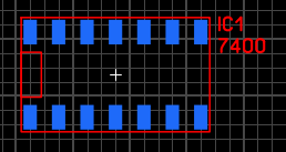
Create a macro for a simple 14-pin DIP-IC.
(This is just an example. Of course, the 14-pin DIP-IC is already included in the macro library.)
1. Draw a macro
We place 14 contacts on the K2 layer (copper-bottom) on the grid with a given pitch. You can change the pad shape for pin1 to define that pad as "Pin 1". To create footprints, it is better to use the “Footprint” function from the “Advanced” menu.
Change the active layer to layer B1 (component layer) and draw the outline of the component near the pins. Use Rectangle mode or another shape mode to draw the outline of the component's body. You can label the drawn component.

The macro is ready. Now you need to select it in order to save it and add it to the macro library.
2. Select elements for the macro
Select all the elements of the created picture by highlighting them with a frame.
All elements of the drawing will be selected.

You can also click on the corresponding button in the macro library.
A dialog box will appear. In this window, select the directory path in the library corresponding to the selected component category. If you want to save the macro in another folder, you need to change the path directory to this folder (directory).
Enter a valid file name for the new macro. The suffix ".lmk" (this is the default suffix for all macros) will be added automatically.
Create component
Components are almost the same as a macro. They contain a set of elements, but in addition they contain a set of special data that allows Sprint-Layout to control the components. Sprint-Layout can create lists of components, and even create a Pick+Place file (for automated placement of SMD components).
Each selected macro can be assigned component data.
To assign data to a macro as a component, click on the macro with the RIGHT mouse button and select the Component... command.
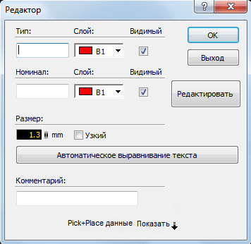
Each component has 2 separate text labels Type (aka ID), we add a serial number to the component type, and Denomination. You can edit these text labels in this editor. You should enter the data carefully as it is used to create the component sheet.
The text will appear on the component layer for the selected macro, but you can also change the layer here.
You can determine the visibility of these text labels. Even if the text is invisible, the data is still available, for example for a list of components.
The Automatic text alignment button automatically aligns 2 text labels, Type (ID) and Denomination, by default, occupying positions at the top/left of the component.
Confirm with OK and the component will be created:

Macro has become a component
If Pick+Place data has been entered for a component, this will be indicated by a small cross in the center of the component.
You can move the text labels Type and Rating to other positions. Click on one of the text labels and move it, while the other text label and component will remain in their position. To select and move another component label, click on it and drag it.
You can call the component editor and edit its data. To open the component editor window, double-click on the component, or RIGHT-click on the component and in the menu window that opens, select the Component... command.
Expand component
You can decompose a component into elements. The component becomes a regular group of elements, but all component data is lost.
To expand a component, call the component editor and click the Edit button.
Modify / Expand Component
Modify an existing component
You can open the Editor window to edit the component. Move the mouse cursor to the selected component and double-click the left button on the component, or right-click on the component and in the pop-up menu, select the Component... command.
Advice:
You can select multiple components and change their details. In this case, each change in the dialog box will be marked in blue. You can assign these highlighted changes to all other selected components after confirming in the dialog box. This way you can, for example, change the text size for all components at once.
Expand component
You can decompose the component at any time. The component becomes a normal group of elements, and all component data is lost.
To expand a component, open the “Editor” window and click the Edit button.
Components in the Macro Library
Once you have selected a macro in the library, you can specify how the macro will be inserted into the project. As a regular macro, or as a component.
If you want to add the selected macros as a component, activate this option As a component in the macro library window, the macro will be added to the project as a component.

Each macro that is selected will be created as a component. After placing the macro on the workspace, the "Editor" dialog box appears automatically and you can change the data, already as a component:
Define data for a macro as for a component directly in the Macro Library
You can edit the component data for a macro directly in the library. Double-click the macro in the preview window and the Editor dialog box will appear. Now you can edit data for the selected macro, as for a component, directly in the library. Each time you use this macro, it will be represented with this data as a component. If you do not use a macro as a component (the option is disabled), its data component will be ignored. The difference between a simple macro and a component is that a macro has no data and cannot be saved to the component sheet, unlike a component. But you can name it by calling the pop-up menu, RIGHT-clicking on the selected macro on the work field, and selecting the “Name” command. This name will be displayed when you hover over a macro installed in the project.
Components sheet
Sprint-Layout can create and manage a list of components that are used in a project. This list is called the Components Sheet.
You can show or hide the component sheet. Click on the corresponding button in the toolbar:
The component sheet will be displayed to the right of the workspace:
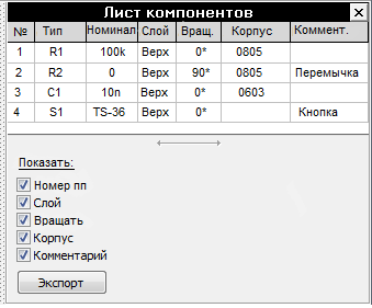
The components sheet contains all the used components of the project that were previously included in the list.
Select a component from this list and the component will be automatically placed on the workspace. Conversely, if you select a component in the project, the corresponding entry in the component sheet will be marked.
You can double-click an entry in the component sheet to open the component editor, and edit the component data.
At the bottom of the component sheet, there are options to show or hide some component data in the list.
When you have checked the options, click on the horizontal arrow, the width of the component sheet will be adjusted automatically, depending on the number of options selected.
Advice:
You can change the width of the component sheet. Move the mouse cursor to the boundary line between the component sheet and the work area. The mouse cursor will change to a double arrow. This means that you can move the border as long as you hold down the left mouse button.
Pick+Place data
The component may contain additional data that is necessary for automated placement of SMD components. This data is called Pick+Place data.
Additional data window:
Rotate component
Component body
Component Center
You can edit this data in an additional window. If you click the Pick+Place data Open button, an additional window opens:
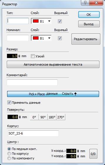
Apply data
This option determines whether the component should have Pick+Place data. Typically, Pick+Place data is only needed for SMD components.
If the component uses Pick+Place data, you will see a small cross in the center of the component. This indicates the use of Pick+Place data for this component.
Turn
You can set the orientation of the component on the workspace.
The rotation determines the angle that the installation machine uses when installing the component onto the board.
Rotation-0 (zero), the component is aligned vertically and its "pin1" and "+" are on top.
If the component is in a different position, the rotation depends on which side of the board the component is installed on. Components on the top side will rotate counterclockwise, and components on the bottom side will rotate clockwise.
In either case, if the component's rotation is set correctly, Sprint-Layout will manage the component's rotation data automatically to rotate the component.
You can edit the component body. For example "SO-8" or "0805_MET". This data is not necessary at all.
The center defines the position that the insertion machine uses when it places the component on the board.
Typically, the center is located exactly in the middle of the component,
You can set the following parameters to define the center:
By copper contacts
Sprint-Layout defines the center as the center of an imaginary rectangle around all SMD pads of the component.
By body
Sprint-Layout defines the center as the center of an imaginary rectangle around all the outline elements of the component body.
By component
Sprint-Layout defines the center as the center of an imaginary rectangle around all SMD pads and all outline elements of the component body.
X/Y coordinates
If the component has an asymmetrical shape, it may be necessary to determine the offset to determine the correct center. The 0/0 button resets this offset to zero.
Export data
Sprint-Layout can export component data to a text file. You can create a list of components or a Pick+Place file, which is necessary for automated placement of SMD components.
To export component data, click the Export... button at the bottom of the “Component Sheet” window:
A dialog box will appear:
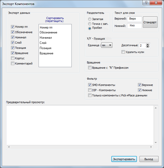
Export data
Here you can define the data that will be exported.
You can also determine the order of data in the list in the right field. Simply drag these values to the desired position.
Separator
Defines the character that will be used to separate data in a string.
Layer text
Defines the side for the component data.
By default, texts are placed in the same way as when placing components on the Top and Bottom sides. The Standard button returns the default text placement.
X/Y - Coordinates
Determine the installation position and format of the specified center.
Rotation
You can determine whether rotation data with the R prefix will be exported or not.
You can select which components should be used for export.
Preview
You can see what the exported data will look like.
Export...
Click this export button to write the data component to a text file.
To print the project, call the Print... command in the File menu, or click the corresponding button on the toolbar:
In the window that opens, you will see a print preview field and options for selecting print options.
In the preview field, you can immediately see what effect for printing this or that selected option will have.

The paper appears as a white page. The red dotted frame indicates the print area on the paper. The area of this zone depends on the printer.
To adjust the print position on the page, move the cursor over the board drawing, click the left mouse button, and move the drawing to the desired position. What you see is what you get!
On the left side of the preview window, there are options:
Here you can select the layers to print. You can define a color for each layer. Click on the color button to the right of each layer. To select a layer, check the box; if the box is not checked, then this layer will not appear on the printout.
You can determine the sequence of layers when printing on a page - 4 buttons below:
The layers are superimposed on one another, starting from the bottom. One image of the board. This is useful when manually scaling, so that you can see all the details of the project on an enlarged printout of the project. Unnecessary layers can be disabled (uncheck the box).
Sequence of printing (overlaying) layers: K2 - I2 - I1 - K1 - B2 - B1 - U
The layers are superimposed on one another, starting from the top. One image of the board. Unnecessary layers can be disabled (uncheck the box).
Sequence of printing (overlaying) layers: K1 - I1 - I2 - K2 - B1 - B2 - U
Prints two images of the board on one page, one below the other. At the top, an image of the board with the upper layers is printed (the overlay sequence is indicated below), and below the second image of the board is printed, but with the lower layers (the overlay sequence is indicated below). Unnecessary layers can be disabled (uncheck the box). When printing two sides on one sheet, be sure to activate the "Board Outline" option, otherwise there will be a very large gap, and the side drawings may not fit into the printable area. It also depends on the board format.
Sequence of printing (overlay) of the top layers (top image): I1 - K1 - B1 - U
Sequence of printing (overlay) of the lower layers (bottom image): I2 - K2 - B2 - U
Prints two images of the board on one page, one next to the other. The image with the top layers is printed on the left, and the image with the bottom layers is printed on the right. The sequence of printing (overlaying) layers is shown below. Unnecessary layers can be disabled (uncheck the box). When printing two sides on one sheet, be sure to activate the "Board Outline" option, otherwise there will be a very large gap, and the side drawings may not fit into the printable area. It also depends on the board format.
Sequence of printing (overlay) of the top layers (left image): I1 - K1 - B1 - U
Sequence of printing (overlay) of the lower layers (right image): I2 - K2 - B2 - U
Additionally
This is a special layer. Here you can define the solder mask and hole list.
Solder mask
The solder mask is created around the solder pads or SMD pads. The diameter (size) of the mask is larger than the contact pad by a certain value. The holes of the contact pads are filled with a mask. Mask 1 – for the top layer. Mask 2 – for the bottom layer.
Using the Settings... button, you can define the properties of the solder mask.
Holes
This option is for printing the diameter and positions of all holes. In the preview window, you can see text marks next to each hole indicating the diameter of the hole.
Using the Settings... button you can determine the height of the text.
Options
Here you can select additional printing options:
Everything is black
Only black and white printing is produced. All colors will be ignored and automatically changed to black.
Mirror
The board (project) will be printed in mirror image. This is necessary for the correct transfer of the design drawing onto the actual board blank. As a rule, the top layers are printed as a mirror image.
Board corners
This option adds 4 crosses to the corners of the board printout to mark its corners.
Circuit
The option puts a frame to show the outline of the board.
Background image
If you have loaded a bitmap image as the background for your project, you can select this option to print that image along with your project.
Negative
Produces a negative imprint. It is used when transferring a pattern onto a photoresist.
Auxiliary mesh
Shows the grid on the preview page. This helps in positioning the print on the paper. The mesh will not print with the project.
Info line
Shows an information line at the bottom of a sheet of paper, printed along with a print of the design. The information line includes: - the name of the project as a whole, the name of the tab in the project, scale, date and time.
This option allows you to scale the printout from 10% to 500%.
1:1 option for printing the drawing in real size.
Orientation
Selecting the orientation of a sheet of paper – Portrait / Landscape.
At the top of the preview, there are additional features:
Automatically places the drawing in the center of the sheet.
To clipboard
Copy the actual image, as a bitmap, to the clipboard. The picture can be inserted into other programs.
Arrangement of several board prints on one sheet, both horizontally and vertically. Enter the number of copies for X-Horizontal and Y-Vertical and the distance between copies.
Correction
Some printers require calibration to produce accurate printouts.
Example: a line is 200 mm long, but the printer prints a line 201 mm long. In this case, enter the correction factor, 200 mm / 201 mm = 0.995. Then the printer will print exactly at the specified scale.
Printer
To select and configure the printer. The selected printer is displayed in the title of the preview dialog box.
Seal
Sending the board design to the printer for printing.
Cancel
Closes the preview window and returns to the working area, without printing.
Export to BMP format
This function creates a bitmap file (*.bmp) that can be used with other applications.
A raster image is created from the layers that are currently visible on the workspace.
To create a raster image file, call the Export -> Format (*.bmp) command in the File menu.

You can choose whether the raster image should be color or black and white.
Quality
Use the slider to adjust the raster resolution. Please note that at higher resolutions ( high quality) requires more memory resources than lower resolutions. Try to reduce the resolution as much as possible with acceptable quality. This is especially important for color raster images.
Export to GIF format
This function creates a GIF file (*.gif) that can be used with other applications.
The GIF is created from the layers that are currently visible on the workspace.
The GIF format is a compressed format, so the resulting file is much smaller than a BMP file.
To create a GIF file, call the command Export -> GIF (*.gif) in the File menu.

Quality
Use the slider to adjust the raster resolution. Keep in mind that higher resolutions (high quality) require more memory resources than lower resolutions. Try to reduce the resolution as much as you can with acceptable quality. This is especially important for color raster images.
Close the dialog box by clicking OK to save the bitmap file.
Export to JPEG format
This function creates a JPEG (*.jpg) file that can be used with other applications.
The JPEG file is created from the layers that are currently visible on the workspace.
JPEG is a file compression format, so the resulting file is much smaller than a BMP file.
To create a JPEG file, call the Export -> JPG (*.jpg) command from the File menu.

Quality
Use the slider to adjust the raster resolution. Keep in mind that higher resolutions (high quality) require more memory resources than lower resolutions. Try to reduce the resolution as much as possible with acceptable quality. This is especially important for color raster images.
Close the dialog box by clicking OK to save the bitmap file.
Gerber-Export
Sprint Layout exports the design to Gerber files with the RS274-X extension, used for professional board production. Gerber files are common to (almost) all manufacturers.
The Gerber file will include all the data for each individual layer in its entirety (copper, components, solder masks, etc.).
Call Export -> Gerber Export... from the File menu to create a Gerber file.
The next window offers several options for creating a Gerber format:

You can select the layer to export. Each layer will be exported to a separate gerber file.
Names for Gerber files
The gerber file name of each layer is displayed next to the layer name. The name of the Gerber file for each side of the board contains 2 parts:
File name + File extension -> Project name_copper (layer name)_bottom (board side).gbr
File name + File extension -> Project name_components (layer name)_top (board side).gbr
In this process, the Filename is the same for all layers and the file extension name will be different for all the layers.
File name:
You can enter a common name for Gerber files. In all files for layers, the Project Name will automatically change.
File extensions...
The file extensions of each layer are predefined. You can change these extensions here:

You can edit extensions for Gerber files.
Mirror
Reflection of the contour layer. This option is mostly unnecessary.
Mirror board outline (board size)
This option adds board size options.
Sverlovka
The option determines where the holes should be drilled. Typically, this parameter is NOT needed. The drilling will be done in any case. This option can be useful if you are drilling holes by hand, but some manufacturers find themselves in a difficult situation if this option is selected.
Centering (0.15 mm)
This option is available in conjunction with the Drilling option. Only center marks of the holes for drilling are applied (punching), which facilitates manual drilling.
Solder Mask Clearance
The options will be available if solder masks are selected. You can separately adjust the gap for a regular pad or an SMD pad. You can choose to export a solder mask for a regular pad and/or an SMD pad (as well as for other elements if they are included in the solder mask).
The solder mask should be slightly larger than the copper element. You can adjust the gap for the SMD pad here.
SMD mask gap
The option will be available if SMD mask is selected. You can adjust the gap for the SMD mask here.
You can see the selected directory for gerber files.
You can change this directory using the Change... button on the right.
Create Gerber file...
Click on the Create Gerber file... button, Gerber files will be created and saved to the folder specified in the directory.
In the list below, you can see a certain protocol for each generated gerber file.
Advice:
Contact the manufacturer to clarify all the circumstances.
Many manufacturers support the Sprint-Layout format (*.lay). In this case, you don't have to create Gerber files yourself. It is enough to provide the manufacturer with your project file.
Excellon-Export
An Excellon file is used by the manufacturer to professionally produce the board for your project. It contains all diameters and hole positions.
To create an Excellon file, call Export -> Hole Data... from the File menu:

You can, either separately or together, choose contact pads with both simple holes and metallized holes.
A separate selection of plating holes is sometimes necessary for professional board production.
Coordinates...
Select which side of the board the coordinates will be created for. If you select to drill from below, the coordinates will be mirrored horizontally.
The Sort by diameter option will sort holes by diameter. This will minimize unnecessary drilling routes.
Unit of measurement
Select coordinate units. Some machines can only handle inches.
The Remove zeros option is usually accepted by machines without problems. If you have problems with this option, you can deselect this option.
Typically, coordinates are exported without a decimal point. The meaning of these coordinates depends on the units of measurement used. Some machines only understand decimal point coordinates. You can select the output option With decimal point.
Special options
These are additional options for the Excellon file.
Milling
Milling is a function for the production of printed circuit boards using special CNC milling machines. Tracks and contacts are cut out on the copper layer of the board. Sprint-Layout supports the milling manufacturing method. Milling data is exported to a plot file in HPGL format (*.plt). Plot file is used by CNC milling machines to produce printed circuit boards.
To create a plot file, call the Export -> Milling data command. (HPGL, *.plt)... from the File menu.
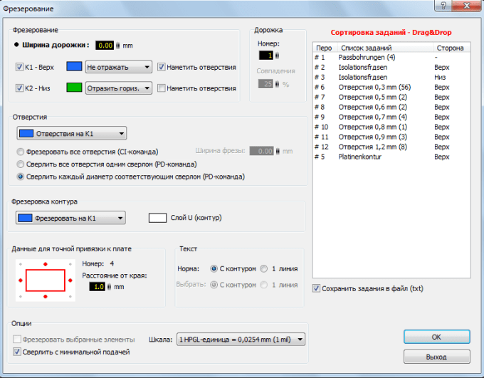
Dialog box for creating a complete plot file.
Milling
Track width
You can specify the width of the milling path. Sprint-Layout uses this width to set the correction parameter for calculating the insulation channels (tracks).
Sprint-Layout cannot define a parameter in such a way as to cut wide, continuous isolation channels between elements. For a milling machine, it is necessary to specify the minimum distance between 2 elements. If the minimum distance is not specified, the insulation channel will not be cut, see the picture on the right:
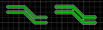
In this case, you can reduce the width of the milling track, but note that all other elements will be slightly smaller if the actual milling tool is larger than the specified milling width.
K1 - Top / K2 - Bottom
You can select the side to be milled.
Typically, the top side is not mirrored and is milled as shown in the actual drawing.
As a rule, the bottom side should be mirrored because it feeds into the machine after the top side. Depending on the order and position (horizontally or vertically) the board will be fed for milling, it is necessary to determine the type of mirror image.
The Mark Holes option helps you mark the centers of the holes for drilling. This option is needed to ensure effective alignment of the CNC drill during the drilling process and reduces the likelihood of breakage of thin and flexible drills at high speeds of the CNC drill.
Only for experts!
By default, the number of milling tracks = 1. You can increase this number to get more insulation channels to increase the milling width.

Holes
You can determine which side to start drilling holes from.
There are 3 options for drilling:
Mill all holes (CI command)
All holes are made with a milling cutter of the same diameter. Holes whose diameter is larger than the diameter of the installed cutter will also be made with the same tool, but will be cut along its circumference, in accordance with the specified hole diameter. A CNC milling machine determines the coordinates of the hole on the board, and the cutter moves around the circle, cutting out a large hole.
Depending on the diameter of the cutter installed, the hole size may be slightly smaller or slightly larger. To prevent this from happening, it is necessary to make a correction to the diameter of the cutter. The “cutter width” option determines the width of the cut line and makes corrections. It is necessary to select a cutter that exactly matches the small diameter of the holes, but not more.
Drill all holes with one drill (PD command)
All holes are drilled with the same drill. Larger diameter holes will only be drilled in the center, i.e. their center is marked. The command is placed in the plot file.
Sprint-Layout will ignore other diameter sizes, and will create one job for all holes.
Drill a new diameter with a new drill (PD command)
The command is written into the plot file as for conventional drilling, but sorted by diameter.
Sprint-Layout will sort all holes by diameter, and writes jobs for each diameter size into one file.
Contour milling
You can determine whether the board outline needs to be milled or not. And also select the side on which you want to mill the contour.
The board outline contains all the lines and arcs indicated on the U layer.
Note:
Data for contour milling is written to the plot file according to its actual size. Depending on the diameter of the installed cutter, the contour size may be slightly smaller or slightly larger. To prevent this from happening, it is necessary to make a correction for the diameter of the cutter, or provide for an adjustment when creating a project in Sprint Layout.
Data for precise reference to the board (helps precise coordination of the board in the machine)
When milling a double-sided board, the board must be precisely coordinated. It is necessary to accurately turn the board over so that there is a complete match when milling. Additional holes are recorded as data for precise reference of board coordinates and transferred to the CNC machine. It is possible to determine whether there are 2 or 3 base holes outside the board. The data for these holes will be written to the plot file as drilling data.
To select additional holes, move the mouse cursor to the field with a red rectangle and gray dots, immediately below the option name. Select the required holes (points), move the cursor over the selected point and click the left mouse button. The gray dot (hole) will change color to red, the hole is activated and will be written to a file. Click the mouse button again to deselect (if necessary) the hole.
The distance of the hole from the edge of the board must also be determined. Set this parameter with the "Edge Distance" option.
The text can be outline or single-track.
Outline text means it will have a milled outline around the text.
Single-track text means that the milled track will be applied along the text itself.
If you need to process texts separately, you must first select (select) the required text, and then select a parameter for it. In this case, you can set different parameters for selected and passive texts.
Mill selected elements
If you select several elements, before calling the Milling window, you need to determine that only these selected elements will be milled.
Drill with minimum feed
Some CNC milling machines may ignore drilling data if they are set to drilling mode with minimum drill feed increments. In this case, you need to activate this option and Sprint-Layout will write a command to control the minimum drill feed.
Some CNC milling machines use rounded scale HPGL units = 0.025 mm (instead of HPGL units = 0.0254 mm). In this case, you can select this scale unit here.
Sorting tasks
On the right are displayed all the tasks according to the specified settings required for the CNC milling machine. The plot file will contain all these tasks in the order they are listed in the task sheet. Sprint-Layout arranges the tasks in the proper sequence, but you can change the order of these tasks as you wish. Rearrange tasks in the desired sequence by simply dragging them.
Create plot file
The generation process may take some time, depending on the complexity of the project.
After this, you will see the creation plan and, as a result, the result for viewing in the project on the workspace. Now you can check the result.

Using this button you can change the width of the milling path. The result can be displayed in the form of thin lines, or a line whose width is written in the task.
The Delete outlines button removes the viewing result from the work field.
General settings
Call the General Settings... command from the Options menu.
You can change all settings for Sprint-Layout.
General settings

Basic settings
In this settings block, you can set the unit of measurement for Sprint-Layout: mm or mil (1 mil = 1/1000 inch).
You can change the units of measurement by clicking on the upper left button in this settings block.
Holes
Can be customized appearance holes. You can select the background color (so that the holes appear transparent), you can set the holes to be displayed in white (for better identification).
Show zoom window
Activates the small green zoom window in the left sidebar, below the tool buttons.
Darken auto-ground layer
The automatic "ground" will appear slightly darker, better differentiated from the rest of the project.
Show all auto-ground layers
You can see all the auto-ground layers on all the copper layers at the same time. If you do not select this option, the auto-ground of the current layer is displayed. Displaying all auto-ground layers at once can be useful, but this option slows down rendering speed, depending on the complexity of the project.
Check connections (elastic) in TEST mode
All elements that are connected by connections (elastic) will be considered.
Flashing TEST mode
The test result is displayed in flashing mode, the connection of elements can be better determined.
CTRL-Test- Capture data of the element being tested
On the selected element, you can view its properties (for example, track width or contact size) in the left toolbar. You can "grab" these values by pressing CTRL while selecting an element, you can use these values for the next drawing. To see these constant values (even without pressing CTRL), you can disable this option.
Limit font line thickness (min. 0.15 mm)
This option limits the text so that the font line thickness is no less than 0.15 mm. This limitation is useful because smaller values cannot be used when making a silk-screened board.
Correctly display markings after element rotation
The text labels TYPE and Rating of a component are always displayed correctly (on the left or bottom), it does not matter if the component is rotated.
Auto-optimization of track nodes
Sprint-Layout removes all duplicate track nodes automatically.
Original mark when exporting (Gerber/Excellon/HPGL)
Typically, a label is used for each CAM export. If you disable this option, the label will be ignored.

You can define your own colors.
There are 4 different color schemes to choose from:
Standard
User 1
User 2
User 3
Standard is a predefined Sprint-Layout color scheme and is not editable.
User color schemes 1..3 are free - editable color schemes that can be changed at your discretion.
To change the color scheme, select "User...". You can change the color of a layer by clicking on the colored square button next to the layer designation.
The Default button resets all custom color schemes and sets the default Sprint-Layout color scheme.
File directories

You can define fixed working folders for various Sprint-Layout files.
When first launched, Sprint-Layout sets default directories for various files.
Using the "..." button, you can select another folder.
Advice:
Leave the field blank if you want to leave the default directory defined by Sprint-Layout.
Option Use one folder for all files, Sprint-Layout will use only one working folder for all files. This option is useful if you are saving files related to the same project.
Library

This is the directory that contains all macros and all additional macro directories.
Using the Change button, you can select another directory, or another macro library, if the folder with macros has been moved, or there is another macro library, but in a different folder.
The Reset button resets the installed directory and sets the default macro library directory.

The "Return" function stores, as a rule, up to 50 steps, which can be undone if necessary. The Revert function remembers 50 actions, but if the project is large, you may need to remember more actions. This is usually not a problem, but if you have your own old PC and notice that the system is running slowly, you may want to reduce the number of memorizations.
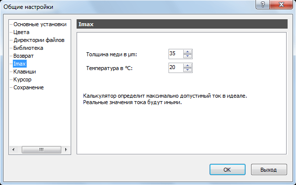
The maximum current selected for the tracks is displayed in the properties panel window.
This value is approximate. The actual value depends on many other factors such as temperature environment, cooling, etc.
There are 2 important parameters for calculating the maximum current for a track: the thickness of the board’s copper (on average 35µm) and the maximum heating temperature (recommended value 20 degrees). You can change these parameters to customize the calculation of the current current value.

You can define new hotkeys for Sprint-Layout drawing tools.
Select the desired drawing tool from the list, and click the arrow in the Change field to select a new key for this mode.
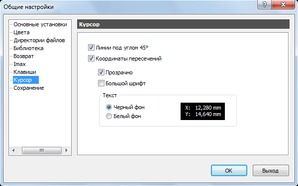
You can make some additional settings regarding the appearance of the crosshair.
Saving

You can increase security when creating a project. You can determine at what time interval the project will be saved automatically. This happens completely in the background and you won't notice it. The periodically saved file will be placed in the same folder and with the same name as the original file, only with a ".bak" extension added to the file name to distinguish it from the original file.
Properties panel
The properties panel provides the ability to edit all important properties of the project and elements, without calling special windows.
To open the properties panel, select Properties panel from the Options menu, or click on the corresponding button on the toolbar:
The properties panel will appear on the right side of the work field.
If no items are selected, only the workspace properties will be displayed:
The properties panel reacts to the current selection on the workspace.
If you select at least one element, for example, one contact, you can change its properties directly here:

You can also edit other elements (tracks, text marks, etc.).
Multi-select
If you select multiple elements, or a group, you can edit the properties of all selected elements at once.
A Multi-Select window will appear at the top of the Properties Panel. Here you can select the type of elements you want to edit. All changes made will be applied to all selected elements.
Design Review (DRC)
When creating a project, some inaccuracies may occur. For the project being created, there are some tolerances and restrictions, these values are called “Design Rules”. To identify all inaccuracies and check design rules, there is a DRC function - control (Design Rule Check). Sprint-Layout can check some important design rules, such as minimum distance between 2 copper traces, etc.
To check, you need to open the DRC Panel.
Select DRC Panel from the Options menu, or click the corresponding button on the toolbar:
The DRC panel will appear on the right.
You can configure DRC parameters. You can select or cancel any of the DRC parameters by checking the box next to the selected parameter, or uncheck it.
Distances:
Between tracks:
Minimum distance between copper traces.
Between holes:
Minimum distance between 2 holes.
Hole diameter Min:
Minimum hole diameter.
Hole diameter Max:
Maximum hole diameter.
Road width Min:
Minimum usable track width.
Ext. hole Min:
Minimal remaining copper ring around the hole.
Component Min:
The minimum usable thickness of a component's outline line.
Labels on contacts:
The option checks whether there are any marks, lines, contours on the pads or SMD pads.
Holes on SMD contacts:
The option checks whether there are holes on the SMD contacts.
Checking for a mask:
The option checks whether there are pins or SMD pins that are not included in the solder mask (can be edited manually).
Checking the mask gap:
The option checks the distance around pins and SMD pins. Can be edited manually.
Start DRC control
Once the test parameters have been selected, you can begin DRC control.
Control
DRC control for the entire project.
Selected
DRC control only the selected part of the project.
If you have made minor changes to the project, you can select this area with changes and check only the selected area.
Test Result (DRS)
After DRC control, all detected errors are listed in the window below. Each entry shows the corresponding layer and the error detected. All errors will be marked in the project with a white, shaded square.

Example: 3 errors (minimum distance)
To display only single errors, select them in the list. You can click the Select All button to select and display all errors.
Advice:
If you double-click on the selected error in the list, it will be automatically enlarged on the working field. You can quickly view each error in a larger view.
Selector
The selector is a powerful tool. Can be used to search and select specific project elements. You can search for and select all contacts of a particular shape or size. Selected elements can be changed in the properties panel.
The selector can also help analyze the project. You can, for example, select all contacts in the Items list and sort them by size. Such lists can help you find unwanted items.
Open the window using the Selector command from the Options menu, or click on the corresponding button on the toolbar:
The Selector panel appears on the right:
Using the top three buttons, with a drop-down menu, you can determine the type of sorting of elements:
Elements:
Select the element type you want to analyze.
Sort by:
Select the sort type you want the Selector to use. The options in this window depend on the selected element type.
You can select elements depending on the layer they are on.
The sorted items will be listed in the form of a list in the window below these buttons.
If you select a group in the list, all elements of this group will be highlighted on the workspace.
If you expand a group, all members of that group will be listed. You can select an individual item rather than the group as a whole.
In combination, Selector and Properties Panel, you can edit the project selectively.
For example, you can select the “contacts” group in the Selector. All contacts in this group will be selected and highlighted on the work field; you can make the necessary changes in the Properties Panel for all contact pads at once.
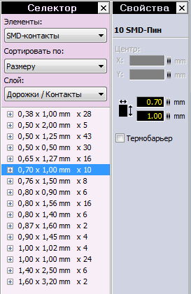
Auto-Scale
Each time you select an entry in the Selector, elements will be selected in the project and Sprint-Layout increments the selected elements. You can change the scale by moving the slider.
Flashing mode of selected items
Selected elements in the project will be highlighted in blinking mode. This will help you identify the selected items. You can disable the flashing mode in the General Settings of Sprint-Layout.
Auto-capture
This feature makes it much easier to connect a track precisely to a pin or other element. As soon as you move the mouse cursor to the selected point, at this moment the cursor will be fixed, and an accurate connection is guaranteed. This function is useful if some connection and contact is not on the same grid scale.
Each time an auto-capture is taken, the cursor is highlighted in red:

Captured crosshair
Auto-capture mode can be turned on or off at any time. Click on the corresponding button at the bottom of the status bar:
Enabled Disabled
Elastic function
When you move elements that are connected by tracks to contacts, the connection connections are preserved. The advantage is that the connections are not broken, but, as a rule, you will have to edit these connections after each such move.
In the Elastic function, you can set one of 3 levels by clicking on the corresponding button at the bottom of the status bar:
Large area Small area Disabled
A large area means that the traces may not be connected to the pins as accurately as when selecting a small area.
The small area means that the trace must be connected exactly in the center of the pad for the connection to be recognized.
You can disable the function, or change the function mode, using the Elastic button.
Footprint Master
The Pad Wizard will help you create component pads.
Select a typical contact scheme and set parameters. The wizard will create pads automatically.
Select Footprint Wizard... from the Advanced menu.

There are 5 different pad installation types available:
Single row (SIP)
Double row (DIP)
Quadruple (QUAD)
Circular
Double circular
Each type of pad has some parameters. These parameters are displayed in the Site Wizard window.
Select the desired contact type from the list. The Standard button sets the parameters to reasonable values, you can see the values of these parameters.
Contacts
You can select the type (regular or SMD) and pad size.
Number of contacts
You can enter the number of contacts.
Options
You can configure the settings that are required for the selected pad type.
Not every parameter is used for every pad type.
The value of each parameter is displayed in the corresponding window, and the result can be seen in the viewing window.
If you click OK, the wizard will create contacts of the specified type and place them on the workspace.
Editing a Solder Mask
Typically, the solder mask will be created automatically in Sprint-Layout.
Sprint-Layout creates a solder mask by excluding all pins and SMD pins from under the mask, so that these areas are free for soldering.
Sometimes it is necessary to change the solder mask. To do this, it needs to be edited.
Click Mask in the left sidebar to enter solder mask editing mode:
All elements that need to be soldered will be displayed in white. As a rule, these are all contacts and SMD contacts.
In this mode, you can add additional elements to the solder mask by clicking on it. This element will be added to the solder mask and will also appear in white.

Conversely, you can exclude the element from the solder mask. Click on a white element to exclude it. The item will be displayed in normal color.
You can reset the solder mask to default values (all pins and SMD pins). To do this, select Default Mask... from the Advanced menu.
Gerber-Import
Gerber files must have the RS274-X extension. The legacy gerber format, with an additional file aperture, is not supported.
Unfortunately, exporting a project to gerber format is not always accurate, as a result of which the imported gerber file may also not accurately display the project. This is because the gerber file is an optical copy of the design. Clear differentiation between tracks, zones or contacts is not conveyed. In addition, each application that creates a gerber file can create this file in its own way. There are many options, but there are no specific rules for creating gerber files. In any case, Sprint-Layout will always try to interpret gerber files, as well as get the best and optimal result.
To create a project from a gerber file, select Gerber-Import... from the File menu.
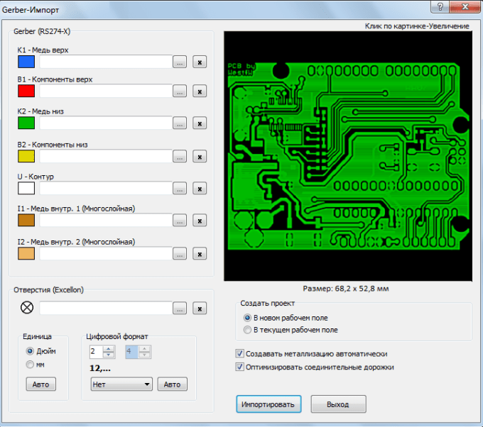
Gerber file (RS274-X)
You can select a gerber file for each layer.
Select a new gerber file using the "..." button. A dialog box will appear where you can select a gerber file.
Please note that if you select a file in the dialog box, that file will be interpreted and the result will be displayed in the main window's preview window. This function is very useful because gerber files often have unclear names by which the contents cannot be recognized. If the file is not recognized as a gerber file, a large X will appear in the preview window. Additionally, if such a file is selected, the file name will be displayed gray, which means the file is not valid.
Hole Data (Excellon)
You can select a hole data file. This file must be in Excellon format.
Sprint-Layout can only automatically recognize this data from an Exellon format file.
By selecting the Exellon file in the dialog box, you will see the hole data in the preview window. The file has additional options regarding digital format. Sprint-Layout recognizes a specific digital file format from Exellon and does not recognize other digital formats. In the dialog box, you can make the necessary changes to the digital file format if you do not know what digital format is used in the file. There are several options you can try. The preview window will always show the result if all settings are correct.
Create a project
You can specify where the project should be created, in a new tab (workspace), or in the current tab (workspace).
Create metallization automatically
Sprint-Layout recognizes through-holes, plated holes automatically. You can disable this feature if activating it produces undesirable results.
Optimize connecting tracks
Sprint-Layout recognizes connecting paths consisting of a single segment to complex combinations of several segments and optimizes them.
Import...
Click Import... to create a project from the gerber file.
Project information
You can open Project Information using the corresponding button on the toolbar:
The Project window will appear:

You can enter information about the project. In the Comment field, you can add an annotation to the project, such as contact information, background information, etc.
Project information will be saved with the project automatically.
Control keyboard
You can control many Sprint-Layout functions from the keyboard:
CTRL key
Hold down the CTRL key on your keyboard to turn off snap to grid, if necessary, place the element at a position outside the grid.
CURSOR keys
Use the CURSOR keys to move the selected elements along the increments of the current grid. If you press the mouse button and the CTRL key, you can move the selected elements in 0.1 mm increments.
SPACEBAR
While drawing a track or zone, you can change the direction, in the “bend” mode, by pressing the key<ПРОБЕЛ>>. There are 5 modes that can be switched with a key<ПРОБЕЛ>.
DEL key
Removes the selected elements from the project.
ALT key
If you want to select one element from a group or macro, press and hold the ALT key and then click on the element you want.
SHIFT key
If you want to select multiple individual items, press and hold the SHIFT key and you can now select one item after another without deselecting the selected items.
F1 key
Calls up help with a description of the program's functions.
F9 key
Activates layers. Only K1 or K2.
F12 key
Automatically replaces the selected simple through-hole contact with a transition contact with metallization.
Hotkeys for modes:
ESC Standard (default)
Z Scale
T Track
P Contact
S SMD contact
Q Rectangle
F Zone (polygon)
N Special shapes
A Auto-trace
M Measurement
V Photo view
O Solder mask
You can change these hotkeys in General Settings.
Keys 1..9
Using keys 1..9 you can select predefined grid values.
Keyboard shortcut:
Cancel
Repeat
Copy
Cut
Insert
Duplicate
Select all
Mirror horizontally
Mirror vertically
Group
Ungroup
Change board side
Information!
Program Sprint Layout 6.0 RUS The program is Russified - Men1. Help for the program, translated and compiled - Sub. Help in testing the Russified version was provided by forum participants: RadioKot.
Somehow I suddenly wanted to describe what I’m doing now.
It just so happens that I mostly draw boards for my own (and others’) electronic designs in the Sprint-Layout program. There is no automation (well, almost none - what we have is very poor) - but I have not yet reached circuits of such complexity that automatic tracers would be needed. Although yes, we should finally master at least one of them. But this is after the rubble at work has been cleared. But I digress. I wanted to talk about how to create your own macro in Sprint-Layout 5.0...
How to create your own macro in Sprint-Layout 5.0 based on a template
Sometimes it happens that among the extensive library of macros (which would not hurt to be thoroughly thinned out!) the required element is not there. But no one is stopping you from drawing it yourself. And here the problem of the size of the installation sites arises. Sometimes these dimensions can be taken from the datasheet, sometimes you have to arm yourself with a ruler. But now I wanted to try to create (in other words, draw) Sprint-Layout macro according to a graphic template.
So, we have a slot for a Micro SD memory card, for which we need a macro.  Most likely you could find a datasheet for it. But there are several types of these connectors, and then anyway, looking at the datasheet, you’ll have to draw all the pads manually. Therefore, we take this connector, place it on the scanner, and scan with a resolution... for example, 600dpi. We get this picture
  We edit it in some way graphic editor, carefully align and save in bmp format. Now Open Sprint-Layout, go to “Options”, “Template...”. Click the “Load” button on any of the tabs (you can work with two templates at the same time, we only need one now, we’re not drawing a board, but a part) and load our saved image. Enter the resolution 600dpi.
 Now we take a ruler and measure any size convenient for us. For example, the width of the connector. I got about 12 mm. The fact is that with the entered 600dpi, we will still get the wrong template dimensions. And in order to adjust the dimensions to the correct ones, we need to focus on something. In the screenshot above you can see the thin green line I have already drawn - its length is just 12mm (to draw it, you may have to turn off snap to grid). It can be seen that the width of the connector on the template is larger than necessary. Therefore, we increase the DPI until we achieve a match between the length of the line and the width of the connector on the template.
 Now you can start drawing. We draw the mounting pads to which the connector body will be soldered. In order to draw contact pads, we will use the “Macro Creator” tool (in the same “Options” menu item). But before that, let’s measure the length of the entire group of pads (the “Measurement” tool on the toolbar on the left).
  Since we have 8 contacts, and 7 spaces between them, we get the distance between the contact pads 7.22/7 = 1.03 mm (in fact, I was wrong - the distance is 7.7 mm, which means the pitch is 1.1, which was basically confirmed by the datasheet). Now “Options” - “Macro Creator”. Select “Single-row SIP”, switch the type of pads from round to rectangular, select their sizes (then you can change them at any time, for example 1.6 and 0.8mm), enter the number of pads (8) and the distance between them 1.03 (correctly 1.1). Click OK and we get a neat row of pads.
  We make sure that we get what we need (the pitch of the pads coincides with the template) and finish drawing the macro to the end. At the same time, we remember that we scanned the connector from the “wrong” side, so do not forget to “mirror” the newly created macro (in Sprint-Layout it is customary to “see” all the details - “from above”, not “from below”).
We got acquainted with the program interface. We'll start the second part of the course by looking at what functions the program for drawing circuit boards provides.
All elements are located on the left panel.
Let's look at them.
Hotkey "Esc".
The default tool. Used to select elements on the workspace. Resetting any tool to the “Cursor” is done by clicking the right mouse button.
Hotkey "Z".
The cursor changes to a magnifying glass. Clicking on the left mouse button on the working field increases the scale of the board, and clicking on the right mouse button decreases it.
Also, with the left mouse button held down, you can select the section of the board that needs to be enlarged.
Hotkey "L".
A tool for drawing a path of a given width. The width value (in mm) is set before starting drawing in the special field below:
The button on the left opens a submenu of frequently used, so-called “favorite” track widths. You can add a new value or remove an existing one:

Note - The item to add a new value becomes active only if the current track width value is not in the list.
After setting the width, selecting the "Path" tool, you can start drawing the path directly. To do this, in the work field, select the point where the line will begin, click the left mouse button and draw the line to the point where it should end.
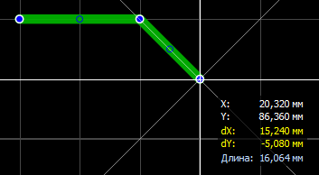
You can change the type of track bend by pressing the Spacebar. Five options are available:
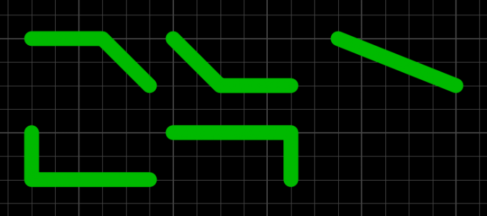
When you press the "Space" key while holding down the "Shift" key, the search is performed in the reverse order.
During the drawing process, you can, if necessary, fix the line by clicking on the left mouse button, thereby forming the required shape of the track.
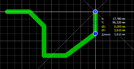
The length value is displayed for the last unfixed segments.
By holding down the "Shift" key you can temporarily make the grid step half as large, and by holding down "Ctrl" you can disable snapping the cursor to the grid.
Having fixed the last point of the track, you can finish drawing the track by clicking on the right mouse button. The track ends and the cursor is ready to draw the next track.
When you select a drawn line, it is highlighted in pink and the properties panel changes appearance, displaying the path parameters:
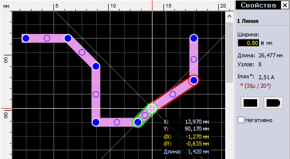
In this panel you can change the value of the line width, view its length, the number of nodes and the calculated maximum allowable current.
Note - Calculation parameters (copper layer thickness and temperature) are configured in the "I max" section of the main program settings (see).
The blue circles represent the nodes of the track. And in the middle of each track segment you can see blue circles - the so-called virtual nodes. By pulling them with the mouse cursor you can turn them into a full-fledged node. Note that during editing, one segment is highlighted in green and the other in red. Green color means that the segment is horizontal, vertical or at an angle of 45°.
The ends of the tracks are round by default, but there are two buttons in the properties panel that make them rectangular (note the left end of the track).
If one trace is represented on the board by two separate tracks and their end nodes are located at the same point, then the tracks can be connected.
To do this, right-click on the end node and select "Connect Line" from the context menu. The track will become solid.

The "Negative" checkbox forms a cutout from the track on the Auto-ground polygon:
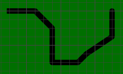
Contact
Hotkey "P".
A tool for creating pads for component pins. By clicking on the small triangle on the left, a contact menu opens where you can select the desired contact form:
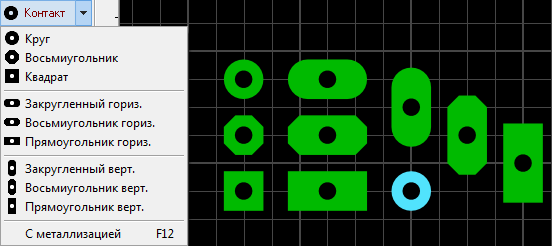
The item “With metallization” makes the contact pad on all layers of copper, and the hole metallized. In this case, the color of the contact with a metallized hole differs from those without metallization (note the round blue contact). The F12 hotkey enables/disables metallization for any selected contact.
The shapes of the contact pads are not limited to this list - they can be made of any shape. To do this, you need to place a regular contact (1), and draw a pad of the desired shape around it (2). Moreover, you should not forget about the mask - you must manually open the entire contact (3) from it (see below about the mask).
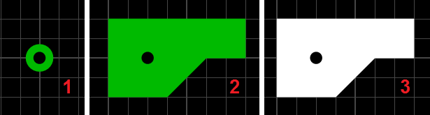
Like the "Track" tool, this tool has its own settings at the bottom:
The upper field specifies the diameter of the contact pad, the lower field specifies the diameter of the hole. The button on the left opens a submenu of frequently used contact sizes. You can add a new value or remove an existing one:
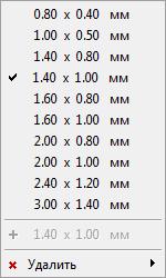
Having set the necessary values, select the “Contact” tool and left-click the mouse to place the contact at the desired point in the working field.
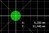
The settings of any selected contact (or group of contacts) can always be changed in the properties panel:
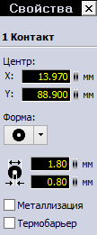
The last item with a checkmark turns on the thermal barrier at the contact. We'll look at this feature in more detail in the next part of the course.
If the contact pad does not have a warranty belt, i.e. The diameter of the hole is equal to the diameter of the contact pad, then it is displayed as follows:

SMD contact
Hotkey "S".
A tool for creating rectangular contacts for surface mount components. Settings:
On the right are fields for entering the width and height of the contact. Below them is a button for changing the values in these two fields. The button on the left opens a submenu of frequently used contact sizes.
Having specified the required dimensions and selected this tool, the contact can be placed on the working field:

For an SMD contact, the thermal barrier function is also available in the properties panel, with the only difference that it can be configured only on one layer.
Circle/Arc
Hotkey "R".
Primitives - circle, circle, arc.
We select the placement point and, holding the left mouse button, move the cursor to the side, thereby setting the diameter of the circle.

Note that the properties panel as you draw contains information about the circle being created. By releasing the left mouse button, we complete the creation of the circle. By selecting it with the "Cursor" tool, we can edit the properties of the circle in the properties panel - in particular, set the coordinates of the center, line width and diameter, as well as the angles of the start and end points if we want to turn the circle into an arc.
You can also turn a circle into an arc by dragging the cursor over the only node on the circle:

The "Fill" checkbox makes a circle out of a circle, filling the inner area, and "Negative", by analogy with a path, turns the element into a cutout on the Auto-ground polygon.
Polygon
Hotkey "F".
A tool for creating areas of any shape. Drawing occurs along a path with a given width:

Once completed, the polygon is displayed with a fill and, when selected, the nodes can be edited (same as in the path tool):
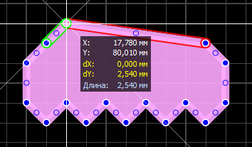
The properties panel contains some more settings:
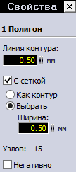
You can change the width of the contour line, see the number of nodes, make a cutout from the polygon using the Auto-earth fill (check “Negative”), and also change the type of polygon fill from solid to mesh.

The thickness of the grid lines can be left as the polygon outline, or you can set your own value.
Text
Hotkey "T".
Text label creation tool. When you select it, the settings window opens:

- Text- input field for the required text;
- Height- text line height;
- Thickness- three various types text thickness;
- Style- text style;
- Turn on- rotate the text to a certain angle;
- Mirror by- reflect text vertically or horizontally;
- Automatically- additionally add a number after the text, starting from a certain value.
Three types of text thickness and three types of style give nine style options (although some are the same):
Note - By default, the minimum possible text thickness is limited to 0.15 mm. If the thickness is too small, the text height is automatically increased. This restriction can be disabled in the program settings menu (see).
Rectangle
Hotkey "Q".
Tool for creating a rectangular outline or rectangular polygon. To draw, click the left mouse button in the work field and, without releasing, move the cursor to the side, setting the shape of a rectangle.
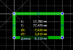
The creation of the rectangle will be completed after the button is released.
As I already said, two types of rectangles are available - in the form of an outline from paths and with a fill.

Moreover, a rectangle in the form of an outline is nothing more than an ordinary path laid in the shape of a rectangle, and a rectangle with a fill is a polygon. Those. Once created, they can be edited as a track and a polygon, respectively.
Figure
Hotkey "N".
Tool for creating special shapes.
The first type of figure is regular polygon:
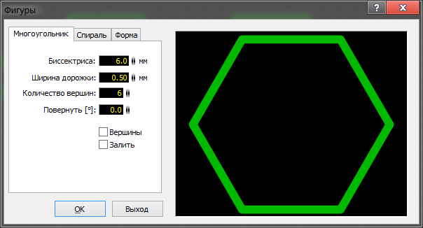
Bisector settings are available - distance from center to vertices, track width, number of vertices, rotation angle.
The "Vertex" checkbox connects opposite vertices to each other ( medium drawing), "Fill" - paints the interior space of the figure (right picture):

It should be noted that the result is elements consisting of tracks and a polygon. Therefore, they are edited accordingly.
The second type of figure - spiral:
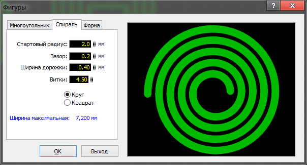
By setting the parameters, you can create a round or square spiral:
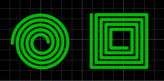
A round spiral consists of quarter circles of various diameters, and a rectangular spiral consists of a track.
The third type of figure - form:
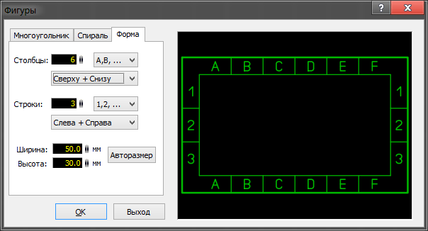
The settings allow you to set the number of rows and columns, the type of numbering, its location, and the overall dimensions of the form. Result:
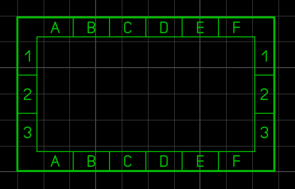
The form also consists of simpler primitives - track and text.
Mask
Hotkey "O".
Tool for working with solder mask. When using it, the board changes color:

The white color of the elements means that the area will be open from the mask. By default, only the contact pads are exposed to the mask. But left-clicking on any element of the current copper layer opens it from the mask (in the picture I opened a path from the mask in the center of the picture). Pressing it back again closes it.
Connections
Hotkey "C".
The tool allows you to establish a virtual connection that is not broken when moving or rotating components between any contacts on the board.
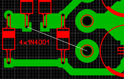
To delete a link, you need to left-click on it with the Link tool active.
Highway
Hotkey "A".
A primitive autorouter. Allows you to trace placed "Connections".
To do this, set the routing parameters (track width and gap) and hover the cursor over the connection (it will be highlighted) and click the left mouse button. If it is possible to lay a route with the specified parameters, then it will be laid:

In this case, the automatically laid route will be displayed with a gray line in the center of the track. This makes it possible to distinguish them from manually laid routes.
Clicking the left mouse button again with the Route tool active on the automatically routed route deletes it and returns the contact link.
Control
Hotkey "X".
The tool allows you to see the entire routed circuit by highlighting it:

Note - in the first part of the course I described setting the type of this backlight: flashing/non-blinking Test mode.
Meter
Hotkey "M".
By holding down the left mouse button, a rectangular area is selected, and a special window displays the current coordinates of the cursor, changes in coordinates along two axes and the distance between the start and end points of the selection, and the diagonal angle of the selection rectangle.
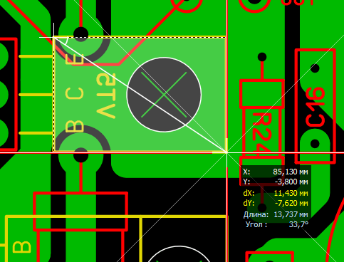
Photoview
Hotkey "V".
A handy tool that allows you to see what the board will look like after manufacturing:


The Top/Bottom switch changes which side of the board is displayed.
Note - The bottom layer when displayed is mirrored compared to the display when tracing. The PhotoView tool works in the same way as if you were twirling a finished board in your hands.
The "With components" checkbox enables the display of the marking layer, and the "Translucent" checkbox makes the board translucent - the bottom layer is visible through it:
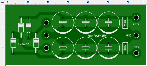
Two drop-down menus - “Board” and “Solder mask” change the color of the mask and the color of the contacts not covered by the mask:

Note - The "---" item displays the contacts as covered with a mask.
Macros
A macro is a saved area boards, ready for further reuse. In Sprint Layout A library of component footprints is organized in the form of macros.
After starting the program, by default the macro panel is open on the right. Opening/closing this panel is controlled by a button on the toolbar on the right side of the window:
This library is currently empty.
To connect the downloaded set of macros, just unpack it and place it in the folder specified in the SL6 settings (see):
After this, the program, having scanned this folder during the next launch, will display macros in the panel:
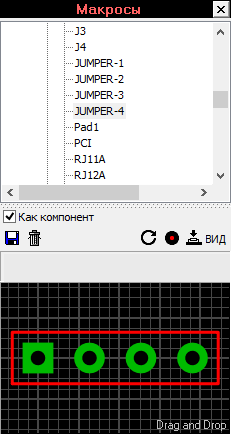
To delete a macro from the library, just select it in the library tree and click on the trash can icon next to the save button.
To edit a macro, you need to drag it onto the work field, make the necessary changes and, having selected the necessary elements, click on the “Save” button and save it as a new macro, giving it a name (or replace the existing one).
IPC-7251 and IPC-7351
I would like to say a few words about naming your macros. There are foreign standards IPC-7251 and IPC-7351, which determine the sizes of contact pads and types of footprints for various standard cases. But in our case, we will need recommendations on naming the footprints from there.
Let's look at the example of a 100 nF capacitor of the B32922 series from EPCOS:
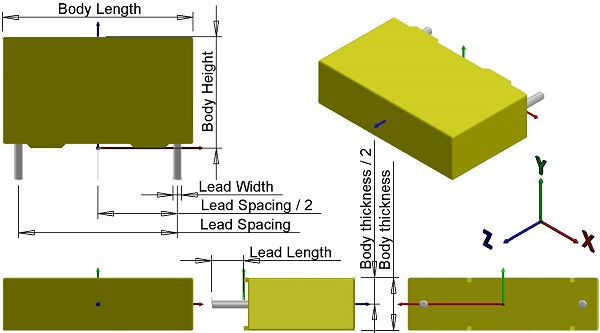
According to the IPC-7251 standard, the name of its footprint will be formed as follows:
CAPRR + Lead-to-pin distance + W Lead thickness+ L Body length + T Case thickness+ H Case height
Therefore, according to the datasheet we have:
CAPRR_1500_ W80_ L1800_ T500_ H1050
CAPRR– Capacitor (CAP), non-polar, radial (R), rectangular (R)
1500
– Pin spacing = 15.00mm
W80– Lead thickness = 0.80mm
L1800– Case length = 18.00mm
T500– Case thickness = 5.00mm
The following parameter is optional - for Sprint Layout it has no meaning:
H1050– Case height = 10.50mm
Thus, this type of naming, after getting used to it, will allow you to find out information about the footprint by the name of the macro and avoid confusion in the library.
I have attached excerpts from the standards to the article:
- Footprint Naming Convention. Surface Mount - for SMD components.
- Footprint Naming Convention. Through-hole - for output components.
Creating Macros
As an illustrative example, we will select a circuit for which we will create a library of macros. Let this be a simple tone control on the TDA1524A chip:
Let's carefully look at the diagram and make a list of components for which we will need macros:
- Chip TDA1524A.
- Fixed resistor with a power of 0.25 W.
- Variable resistor.
- Electrolytic capacitors.
- Film capacitors.
- Connectors for connecting power, as well as for connecting a signal source and load.
- Miniature switch.
The process of creating a macro consists of several steps:
- Arrangement of contacts.
- Drawing graphics for the marking layer.
- Saving the macro in a separate file on disk.
In the video below I will show you the process of creating macros for elements of the selected diagram in two ways.